
| Home | S-100 Boards | History | New Boards | Software | Boards For Sale |
| Forum | Other Web Sites | News | Index |
 |
 |
 | |
| Intel 80486 CPU |
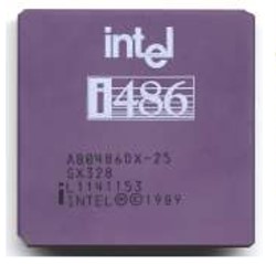
| Intel 80486-DX | ||
| This CPU ran with core a frequency equal to bus frequency, introduced in May 1990. It was followed in June 1991 by the DX-50. Both chips at full speed ran hot. To run the DX-50 at 50MHz required a heat sink. To over-clock this chip, it required a heatsink-fan, with that it could run all day long at 60MHz. At the speed we run the CPU on our S100 board no heat sink is required. | 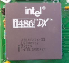 |
| Intel 80486-DX2 | ||
| This chip was very popular with OEMs and system builders. The CPU internally ran at 2X the speed of the external bus. Unlike the DX-33 and DX-50, the DX2-50 didn't require a heat sink for use. Also unlike the DX series , the DX2 series didn't require OEMs to build quality advanced high speed clocked circuits throughout the motherboard. It was introduced in March 1992 | 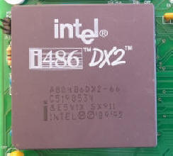 |
| Intel 80486-DX4 | ||
The 80486DX4 continued the trend started by the 80486DX2 toward faster clock speed processors on slower motherboards. The DX4 uses "clock tripling", where the processor runs at three (not 4), times the speed of the memory bus (motherboard). Intel's DX4 ran internally at two speeds: 75 MHz (for the 25 MHz bus) and 100 MHz (for the 33 MHz), with the 100 being by far the most popular. In order to keep power and heat to a manageable level the voltage of these chips was reduced to 3.3 volts. The Intel, AMD and Cyrix versions of the DX4 chip are quite similar. One difference was that the AMD and Cyrix support write-back cache while the Intel did not; however the Intel had its level 1 cache doubled to 16 KB. All three chips supported power management. The chip was first introduced in March 1994. | 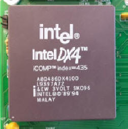 |
| Intel 80486-SX | ||
The Intel 80486SX is the same chip as the 80486DX with one exception: the lack of an integrated math coprocessor BTW, this is a different kind of difference between the SX and DX versions than is the case with the 386; the 386SX and 386DX both had no coprocessor and the 386SX had narrower data and address buses than the 386DX. The 486DX and 486SX have the same bus widths. Since it is the same chip except for the floating point processor, the 486SX had all the same advantages over the 386 that the 486DX had. The 486SX was available in slower clock speeds than the 486DX; the SX came in 16, 20, 25 and 33 MHz versions, while the DX came in 25, 33 and 50 MHz versions. The 486SX was a popular choice for laptops due to its lower cost and lower power consumption. The SX was introduced in April 1991. | 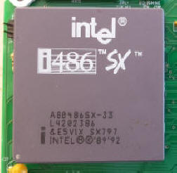 |
| AMD 5X86 | ||
Not introduced until November 1995, the AMD 5x86 was a standard 486 processor with an internally-set multiplier of 4, allowing it to run internally at 133 MHz on systems with clock-multiplied DX2 or DX4 486 processors. Like most of the later 486 parts, the 5x86 featured write-back L1 cache, and unlike all but a few, it had a generous 16 kilobytes rather than the more common 8KB. | 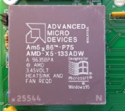 |
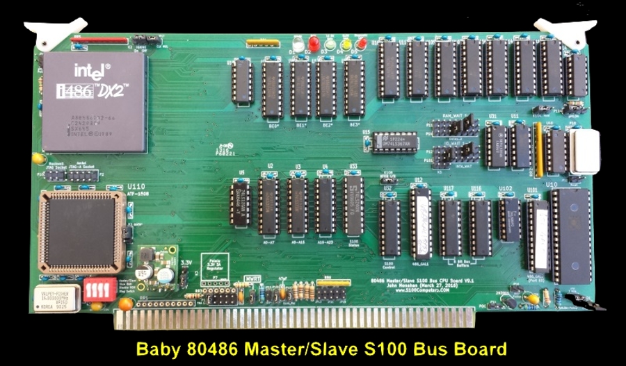
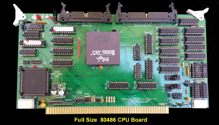
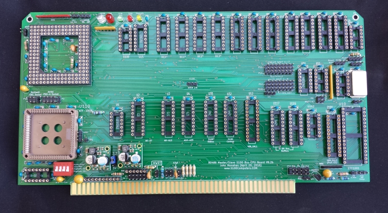
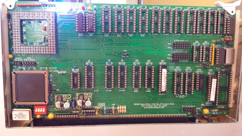
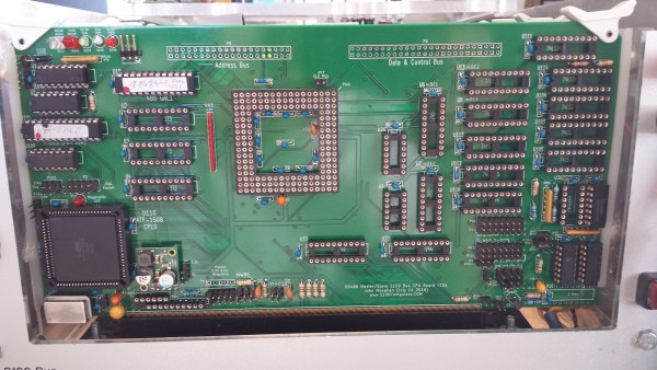
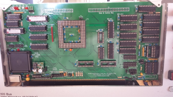
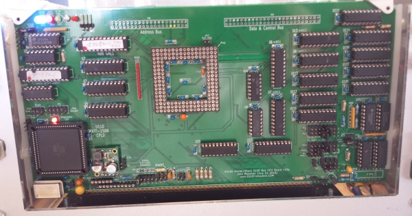
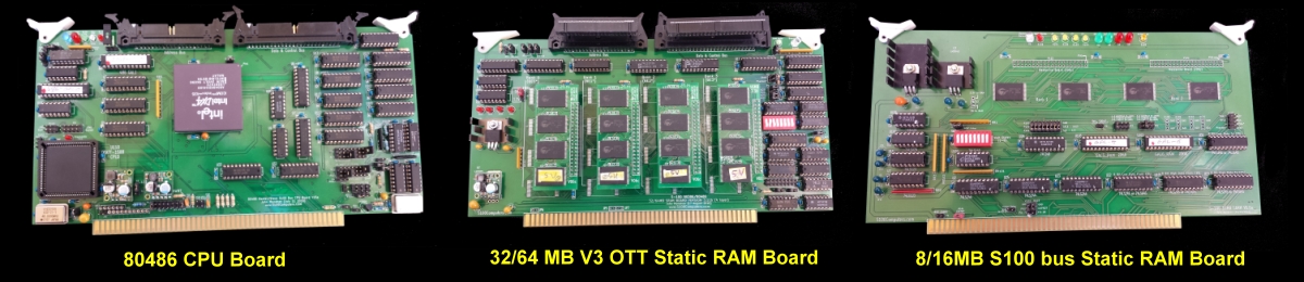
| 1 | Build and debug a Master/Slave S-100 80486 CPU board such that it is completely self-contained and can run MS-DOS in the system on the S-100 bus. Using only an 8 bit S100 data bus | |
| 2 | Build and debug a Master/Slave S-100 80486 CPU board such that it is completely self-contained and can run MS-DOS in the system on the S-100 bus. Using both an 8 and 16 bit S100 data bus | |
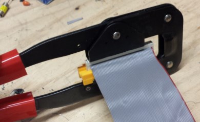
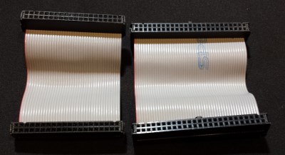
| 3 | Build a ribbon cable connected S100 daughter RAM board utilizing very high capacity static RAM chips (16M chips). | |
| 4 | Build the same type of board utilizing very high capacity DRAM SIMMS (1GB SIMMS). |
 |
 |
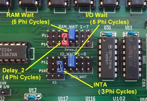 | |
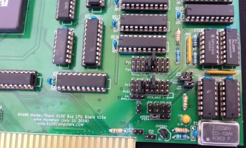
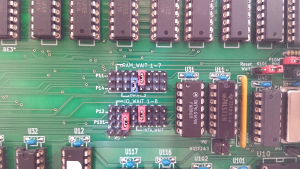
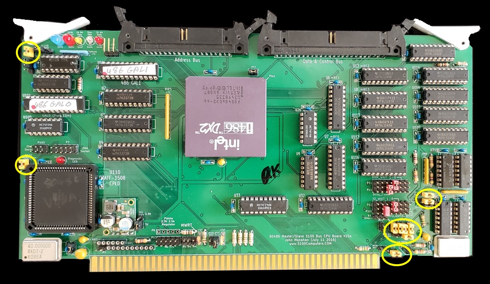
| Baby 80486 Wait State Jumpers |
 |
 |
 |
 |
 | |
 |
 |
 |
 |
 |
 |
 |
|
 |
 |
 |
|
|
 |
 |
|
|
 |
 |
 |
|
 |
|
|
 |
 |
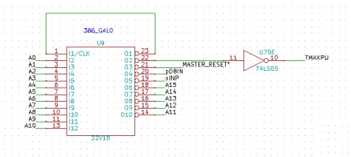
Problem 1 – Master/slave switching when performed by input from
port EDh.
This option has been implemented on all slave CPUs using a GAL or CPLD
with inputs obtained directly from the S100 bus. The trigger to enable (and
disable) the slave CPU is simply an INPUT to port EDh, allowing master/slave
switching under software control without the need for a System Monitor
Board. Some of John Monahan’s older software (specifically, CPM86+) also
depends on this method to switch in the x86 slave processor.
The problem I encountered was that the switching circuit was being
triggered randomly while running either CPM3 on the Z80, or MSDOS on the
80486. This “random trigger” issue was previously mentioned by Jay Jaeger
when he encountered it on the S100 PDP-11 board, where the required logic is
implemented within one of the board’s CPLDs:
https://groups.google.com/g/s100computers/c/afLCbpQG1B4/m/VeqL7SXlCwAJ
It seems this switching logic is very sensitive to noise on the S100 bus
– in my case, the problem went away when I removed an S100 extender board
that had been plugged into the last slot of the backplane.
Problem 2 – Master/slave switching when performed by lowering
TMA0-3 using the System Monitor Board
The problem I encountered was that when master/slave switching was
performed under software control using the SMB, all four of the TMA lines
would become active at the same time even though the data output to port EEh
was to to lower only TMA0. When performed manually (from the Z80 system
monitor) the circuit always performed correctly. This issue has been
previously described here by Gary Milliorn when using the 68030 CPU, and by
Michael Wachur who presented a detailed analysis of the cause of this
problem when using the 80486 CPU:
https://groups.google.com/g/s100computers/c/nqoK8Q3Hyk4/m/fx85IhDRGAAJ
https://groups.google.com/g/s100computers/c/iBmkGTRDi_Y/m/_lk8Kvm3AAAJ
The cause is related the design of the SMB, which latches its address
lines to improve the appearance of its hex displays. When the SMB is
used with very fast CPUs the latched address provided to the address decoder
for the TMA port select circuitry is that of the previous bus cycle –
resulting in incorrect data being saved into the register storing the bits
controlling the four TMA lines. Gary and Michael solved the problem (using
different methods) by delaying the slave CPU generation of the bus write
control signal. I decided not to mess with the 80486 or 68030 boards, and
instead opted to “fix” the design of the SMB. I replaced the SMB’s LS273
address latches with LS373s that have their control inputs jumpered so the
LS373s simply function in “data pass through” mode. This completely solves
the problem with the TMA select logic, and avoids the potentially disastrous
consequences of having the bus master and all slave boards going active
simultaneously.
This page was last modified on 07/06/2022